YOUR BROWSER IS OUT-OF-DATE.

We have detected that you are using an outdated browser. Our service may not work properly for you. We recommend upgrading or switching to another browser.

Department of Nanometrology

Research

Our research areas

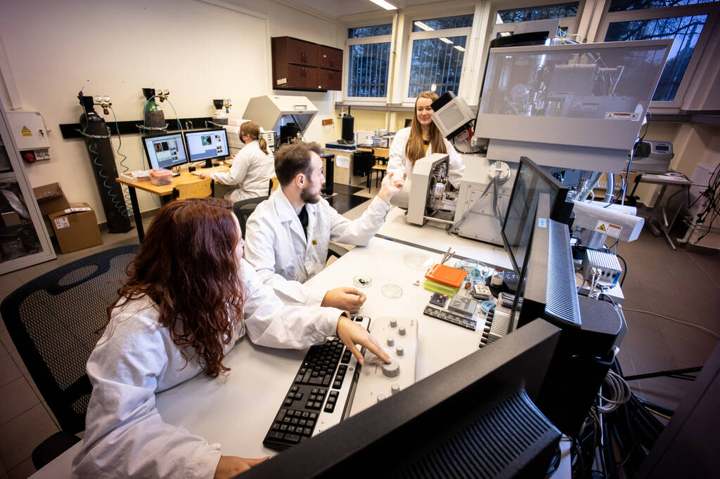
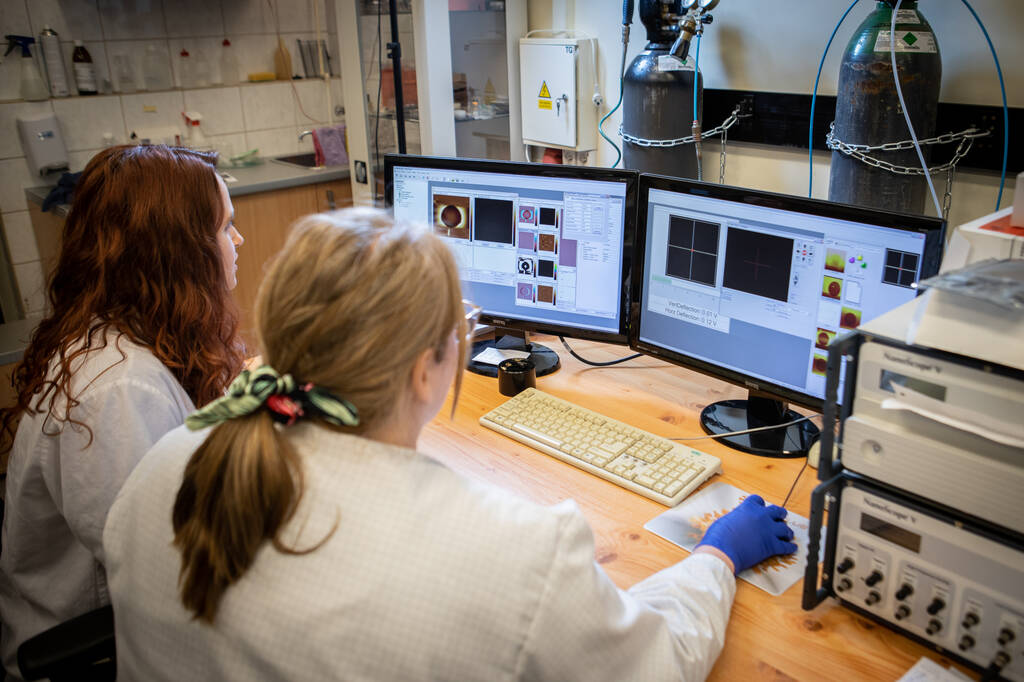
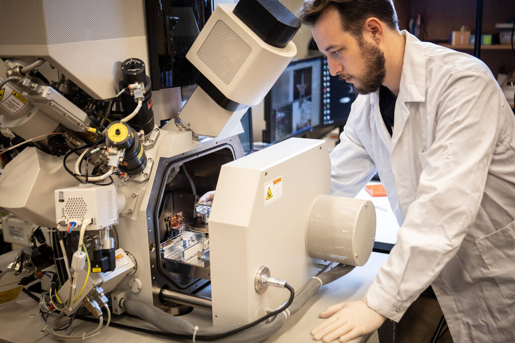
We are focused on investigating of various nanometrology aspects involving the utilization of Atomic Force Microscopy, Scanning Electron Microscopy a Focused Ion Beam. We design, implement, and test various measurement techniques and setups, based on advanced electronic circuitry consisting of embedded processors and FPGA platforms. We cooperate with variety of research institutions in Poland and worldwide.

Gallery

The Laboratory of Nanometrology and Nanofabrication with Focused Ion Beam and Electrons

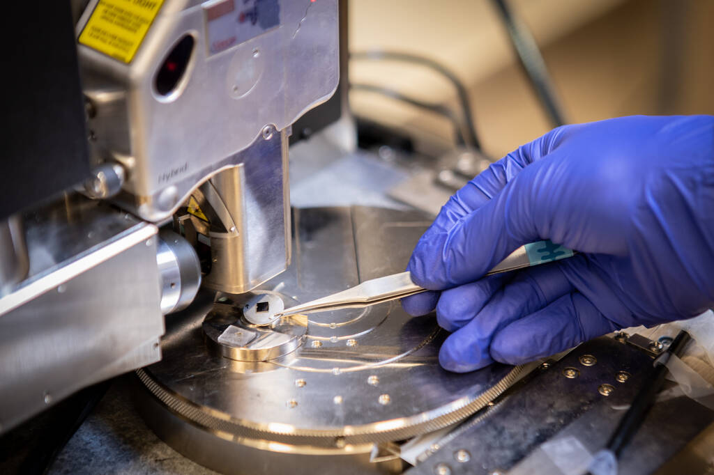
We perform advanced micro-and nanoscale experiments using Lab-in-SEM approach. The experimental procedures involve fabricari9o

The equipment:

  • Dual beam system Helios NanoLab 600i – scanning electron microscope with focused ion beam provides the samples imaging, deposition and etching of the nanostructures, ion implantation into the material, electrical and optical measurements. The parameters: the proces resolution – less than 10 nm, acceleration voltage for the electrons and focused ion beam: 350 V – 30 kV.
  • Plasma cleaning system, plasma deposition system, optical microscopes.

The examples of the publications: 

  • https://doi.org/10.1016/j.mee.2017.03.009 
  • https://doi.org/10.1016/j.micron.2019.102792 
  • https://doi.org/10.3390/s19204429 
  • https://doi.org/10.1016/j.measurement.2021.110373 
  • https://doi.org/10.24425/mms.2020.131710 

Gallery

The Laboratory of Near Field Microscopy

The investigations of various properties of the samples at micro- and nanoscale are performed. The determination of morphological, mechanical, electrical, magnetic, thermal and piezoelectrical properties is carried out using a variety of the measurement modes of atomic force microscopy.

The equipment:

    Atomic force microscopes:

  • atomic force microscope Veeco/ MultiMode V
  • atomic force microscope Dimension 3100
  • home-made atomic force microscope dedicated to the measurements of the electrical properties of the nanostructures,
  • home-made atomic force microscope dedicated to the measurements of the thermal properties of the surface, scanning electron microscope (STM)

    Available imagin modes/ techniques:

  • STM - Scanning Tunelling Microscopy,
  • contact mode, semicontact / TappingMode,
  • LFM - Lateral Force Microscopy,
  • MFM - Magnetic Force Microscopy,
  • EFM - Electrostatic Force Microscopy,
  • KPFM - Kelvin Probe Force Microscopy,
  • SSRM - Scanning Spreading Resistance Microscopy,
  • FMM - Force Modulation Microscopy,
  • PFM - Piezoresponse Force Microscopy,
  • FS - Force Spectroscopy.

 The examples of the papers:

Gallery

The Nanometrology Laboratory of the Structures and Electronic Materials

We conduct the research in the field of modern low-dimension structures. The development and determination of electrical and mechanical structures made of two-dimensional materials are performed.

The equipment: 

2D materials transfer setup integrated with the optical microscope stand-alone setup for the 2D materials transfer transmission and reflectance spectroscopy setup

The examples of the papers: 

Gallery

The Laboratory of the Material’s Electrical Tests

We perform:

  • The impedance spectroscopy tests in frequency domain.
  • Determination of the impedance of biological and biochemical structures
  • The analysis of electrical properties of electrical, optoelectronic, micro- and nanoelectronic devices
  • The interpretation of the results of AC measurements, using various equivalent models
  • Determination of the properties of dielectric materials, in particular the current conduction mechanism in dielectrics and nanocomposites

The examples of the papers:

  • https://doi.org/10.3390/v12040407 
  • https://doi.org/10.1016/j.sna.2019.111747 
  • https://doi.org/10.1016/j.measurement.2016.05.057 
  • https://doi.org/10.1088/0957-0233/26/6/065002 
  • https://doi.org/10.1016/j.snb.2014.12.105 
  • https://doi.org/10.1016/j.snb.2011.08.020

The Laboratory of the Implementation of Microcontrollers, Programmable Logic and Signal Processors

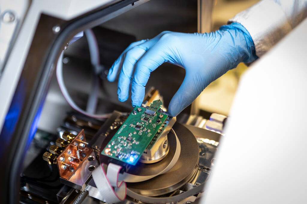
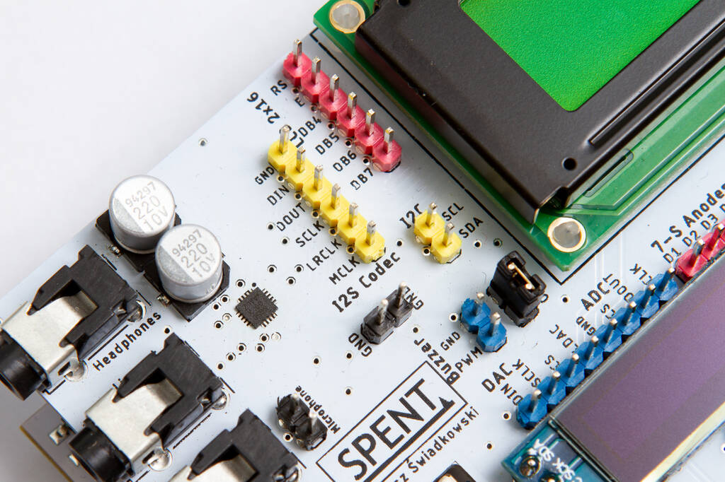
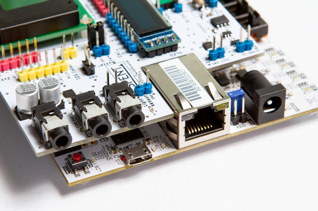
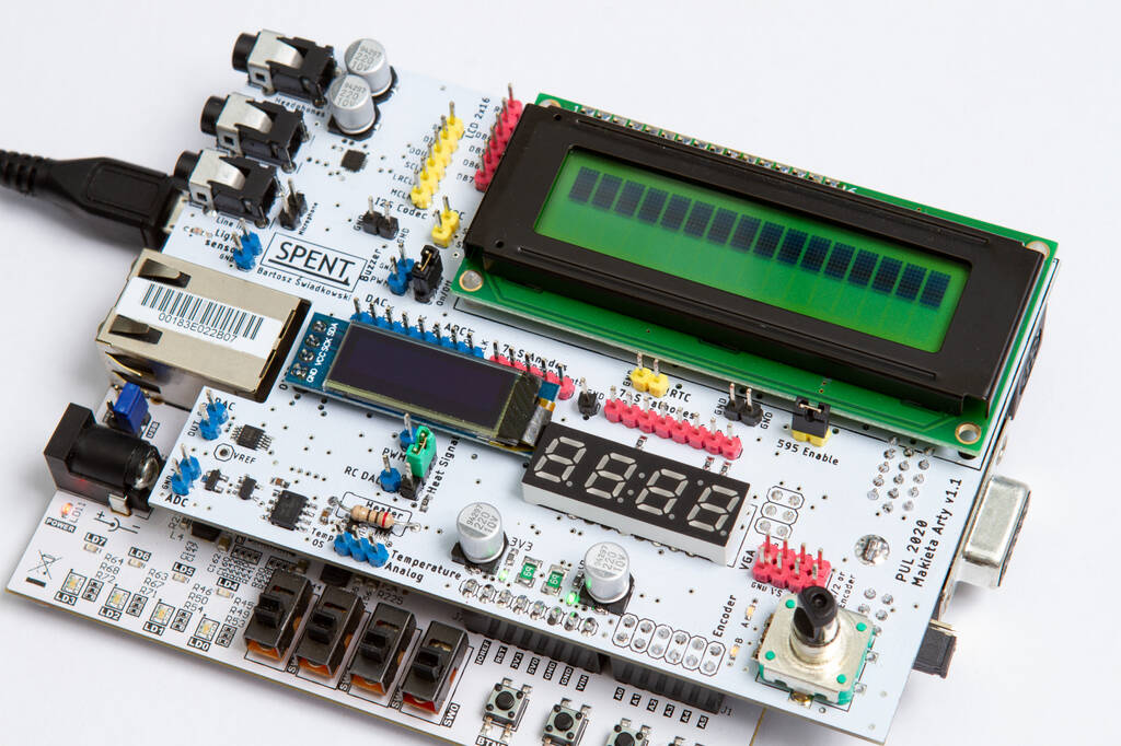
We perform the microcontrollers programming and hardware accelerators for research equipment, including the signals acquisition systems, involving their full characterization and processing of obtained data. The development of physical prototypes (complete PCB, including BGA footprint IC’s), and programming of FPGA Xilinx and Intel, as well as the ARM architecture (Cortex-M, Cortex-A).

Gallery

The Laboratories of Optical Fiber Sensors and Optoelectronics

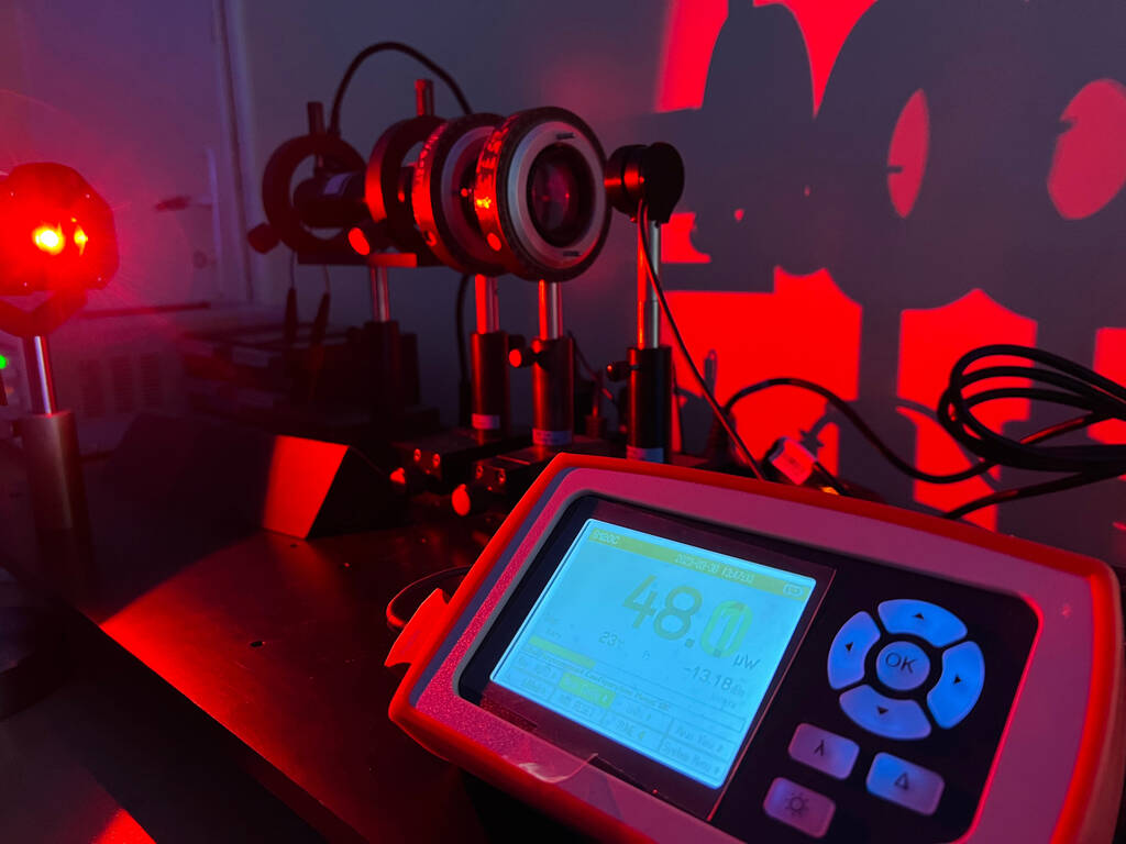
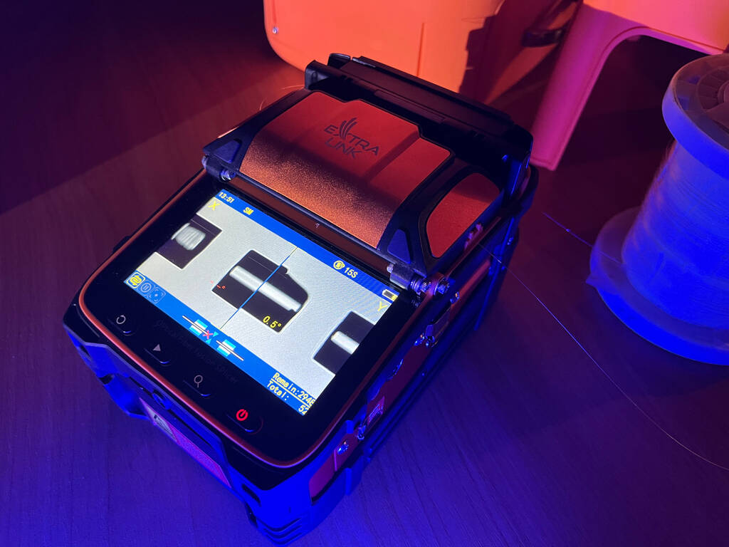
We perform various experiments in the field of development of optical fiber sensors and measurement devices applicable in wide range of industry, technology and research, in particular, in the field of nanoscale diagnostic.

The equipment:

  • The optical spectrum analyzer ANDO AQ6315B  provides advanced measurements including the light source evaluation and spectral analysis of the optical devices. The measurement range: 350 nm do 1750 nm.
  • The optical interrogator NBG FBGUARD 1550 enables the data readout from optical fiber sensors with Bragg grating (FBG) used in static and dynamic monitoring. The device provides the measurements from the network of the sensors of various properties (deflection, temperature, displacement or acceleration). The measurement spectral rang is in range of 1530-1570 nm, and sampling range 200 kHz.

Two laser vibrometers (SIOS Meßtechnik GmbH) working in the Michelson’s interferometer setup, are used for the determination of mechanical properties of the microstructures in the air and vacuum.

Two vacuum chambers with electrical connectors provide the tests in controlled environment, one provides cryo experiments.

The optical setups with optical fibers implementation option stand.

The examples of publications:

  • https://doi.org/10.1088/1361-6501/ac3678 
  • https://doi.org/10.1016/j.measurement.2021.110373 

Gallery

Politechnika Wrocławska © 2025